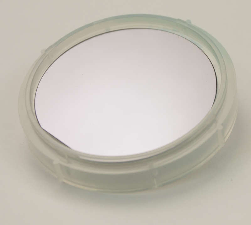
InP Single crystal substrate
InP Single crystal material is one of the most important compound semiconductor materials, which is the key material in optical fiber communication technology. Based on InP, laser diode (LD), light-emitting diode (LED) and photodetector realize the functions of information transmitting, transmitting, amplifying and receiving in optical fiber communication. InP is also very suitable for high frequency devices, such as high electron mobility transistor (HEMT) and heterojunction bipolar transistor (HBT). Due to its advantages, InP has been widely used in many high-tech fields, such as optical fiber communication, microwave, millimeter wave, anti radiation solar cell, heterocrystal tube and so on
Growth method
Liquid seal extraction LEC
crystal structure
cube
Lattice constant (nm)
0. 587
Crystallographic orientation
< 100 >, < 110 >, < 111 > ± 0.5 º, or special direction
Doping degree
Light, medium and heavy admixtures
Dopant element
Undoped
S-doped
Zn doping
Te doping
Conductive type
N
N
P
N
Band gap (EV)
one point three four
Resistivity (Ω· cm)
Mobility (cm2 / (V · s))
(3.5-4)×103
(2.0-2.4)×103
(1.3-1.6)×103
70-90
≥2000
Carrier density (/ cm3)
(0.4-2)×1016
(0.8-3)×1018
(4-6)×1018
(0.6-2)×1018
107-108
Dislocation density (EPD) (/ cm2)
<5×10⁴
3×10⁴
2×10³
2×10⁴
3×10⁴
size
Φ 2 ″× 0.5mm, Φ 3 ″× 0.5mm, special direction and size can be customized according to customer requirements
surface
Single, double or cutting
Thickness (UM)
500, thickness tolerance + - 10um, customizable
TTV (Total Thickness
Variation)
TIR (Total Indicated
Reading)
Bow
Warp
packing
Class 100 clean bag, class 1000 super clean room
供应磷化铟InP单晶基片 厂家品牌_深圳泛美金属 欢迎广大客户来电咨询洽谈交易,18928450898
磷化铟InP单晶基片
InP单晶材料是最重要的化合物半导体材料之一,是光纤通信技术中的非常关键的材料,基于InP的激光二极管(LD)、发光二极管(LED)和光探测器等器件实现了光纤通信中信息的发射、传播、放大、接受等功能。InP同时也非常适用于高频器件,如高电子迁移率晶体管(HEMT)和异质结双极晶体管(HBT)等方面。由于InP本身具有的优越特性,使其在光纤通信、微波、毫米波、抗辐射太阳能电池、异质结晶体管等诸多高技术领域有着广泛的应用.
|
生长方法
|
液封提拉法LEC
|
|
晶体结构
|
立方
|
|
晶格常数(nm)
|
0. 587
|
|
晶向
|
、、±0.5º、或特殊方向
|
|
掺杂程度
|
轻掺、中掺、重掺
|
|
掺杂元素
|
不掺杂
|
掺S
|
掺Zn
|
掺Te
|
|
导电类型
|
N
|
N
|
P
|
N
|
|
带隙(eV)
|
1.34
|
|
电阻率(Ω·cm)
|
|
|
|
|
|
|
迁移率(cm2/(v·s))
|
(3.5-4)×103
|
(2.0-2.4)×103
|
(1.3-1.6)×103
|
70-90
|
≥2000
|
|
载流子密度(/cm3)
|
(0.4-2)×1016
|
(0.8-3)×1018
|
(4-6)×1018
|
(0.6-2)×1018
|
107-108
|
|
位错密度(EPD)(/cm2)
|
<5×10⁴
|
3×10⁴
|
2×10³
|
2×10⁴
|
3×10⁴
|
|
尺寸
|
Φ2″×0.5mm、Φ3″×0.5mm,可按照客户需求,定制特殊方向和尺寸
|
|
表面
|
单抛片、双抛片或切割片
|
|
厚度(um)
|
500,厚度公差+-10um,可定制
|
|
TTV (Total Thickness
Variation)
|
|
|
TIR (Total Indicated
Reading)
|
|
|
Bow
|
|
|
Warp
|
|
|
包装
|
100级洁净袋,1000级超净室
|


 NEWS
NEWS