As a substrate, indium arsenide InAs single crystal substrate can not only grow InAsSb / in aspsb, innassb and other heterojunction materials, but also be used to fabricate infrared light-emitting devices with wavelength range of 2-14 μ m, epitaxial growth of AlGaSb superlattice structure materials, and fabrication of mid infrared quantum cascade lasers. Infrared light-emitting devices and infrared lasers have very good application prospects in gas monitoring, low loss fiber communication and other fields. InAs single crystal has high electron mobility and is also an ideal material for Hall devices.
Growth method
Liquid seal extraction LEC
crystal structure
cube
Lattice constant (nm)
zero point six zero six
Crystallographic orientation
< 100 >, < 110 >, < 111 > ± 0.5 º, or special direction
Doping degree
Dopant element
Undoped
Sn doping
Zn doping
S-doped
Conductive type
N
N
P
N
Band gap (EV)
zero point three five four
Resistivity (Ω· cm)
Mobility (cm2 / (V · s))
2×10⁴
>2000
100-300
>2000
Carrier density (/ cm3)
5×10¹⁶
(5-20)×1017
(1-20)×1017
(1-10)×1017
Dislocation density (EPD (/ cm2)
<5×10⁴
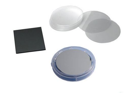
size
Φ 2 ″× 0.5mm, Φ 3 ″× 0.5mm, special direction and size can be customized according to customer requirements
surface
Single, double or cutting
Thickness (UM)
500, thickness tolerance + - 10um, customizable
TTV (Total Thickness
Variation)
TIR (Total Indicated
Reading)
Bow
Warp
packing
Class 100 clean bag, class 1000 super clean room
供应砷化铟InAs单晶基片 厂家品牌_深圳泛美金属 欢迎广大客户来电咨询洽谈交易,18928450898
InAs单晶作为衬底,不仅可以生长InAsSb/In-AsPSb、InNAsSb等异质结材料,用来制作波长范围为2~14μm的红外发光器件,还可以外延生长AlGaSb超晶格结构材料,制作中红外量子级联激光器。红外发光器件和红外激光器在气体监测、低损耗光纤通信等领域有非常好的应用前景。InAs单晶同时具有很高的电子迁移率,也是一种制作Hall器件的理想材料。
|
生长方法
|
液封提拉法LEC
|
|
晶体结构
|
立方
|
|
晶格常数(nm)
|
0.606
|
|
晶向
|
<100>、<110>、<111>±0.5º、或特殊方向
|
|
掺杂程度
|
|
|
掺杂元素
|
不掺杂
|
掺Sn
|
掺Zn
|
掺S
|
|
导电类型
|
N
|
N
|
P
|
N
|
|
带隙(eV)
|
0.354
|
|
电阻率(Ω·cm)
|
|
|
|
|
|
迁移率(cm2/(v·s))
|
2×10⁴
|
>2000
|
100-300
|
>2000
|
|
载流子密度(/cm3)
|
5×10¹⁶
|
(5-20)×1017
|
(1-20)×1017
|
(1-10)×1017
|
|
位错密度(EPD(/cm2)
|
<5×10⁴
|
|
尺寸
|
Φ2″×0.5mm、Φ3″×0.5mm,可按照客户需求,定制特殊方向和尺寸
|
|
表面
|
单抛片、双抛片或切割片
|
|
厚度(um)
|
500,厚度公差+-10um,可定制
|
|
TTV (Total Thickness
Variation)
|
|
|
TIR (Total Indicated
Reading)
|
|
|
Bow
|
|
|
Warp
|
|
|
包装
|
100级洁净袋,1000级超净室
|


 NEWS
NEWS