

 单质
单质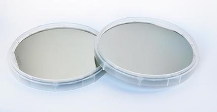


典型规格见下表
Semi-conducting Ge Specifications
| Growth Method | VGF |
| Dopant | n-type: As; p-type: Ga |
| Wafer Shape | Round (DIA: 2" 4" 6") |
| Surface Orientation** | (100)±0.5° |
**Other Orientations maybe available upon request
| Dopant | As (n-type) | Ga (p-type) |
| Resistivity (Ω.cm) | 0.05-0.25 | 0.005-0.04 |
| Etch Pitch Density (cm2) | ≤ 300 | ≤ 300 |
| Wafer Diameter (mm) | 50.8±0.3 | 100±0.3 |
| Thickness (µm) | 175±25 | 175±25 |
| TTV [P/P] (µm) | ≤ 15 | ≤ 15 |
| WARP (µm) | ≤ 25 | ≤ 25 |
| IF* (mm) | 17±1 | 32.5±1 |
| OF (mm) | 7±1 | 18±1 |
| Polish** | E/E, P/E, P/G | E/E, P/E, P/G |
| Backside Ra (µm)*** | < 0.1 | < 0.1 |
``````````````````````更详细要求请来电咨询!``````````````````````````